

Design for Testability (DFT)
DFT techniques improve the testability and manufacturability of semiconductor devices by enabling efficient detection of manufacturing defects.

We design and verify the silicon that powers tomorrow's vehicles, connectivity, and intelligent edge, from architecture through tape-out and bring-up.
DFT techniques improve the testability and manufacturability of semiconductor devices by enabling efficient detection of manufacturing defects.
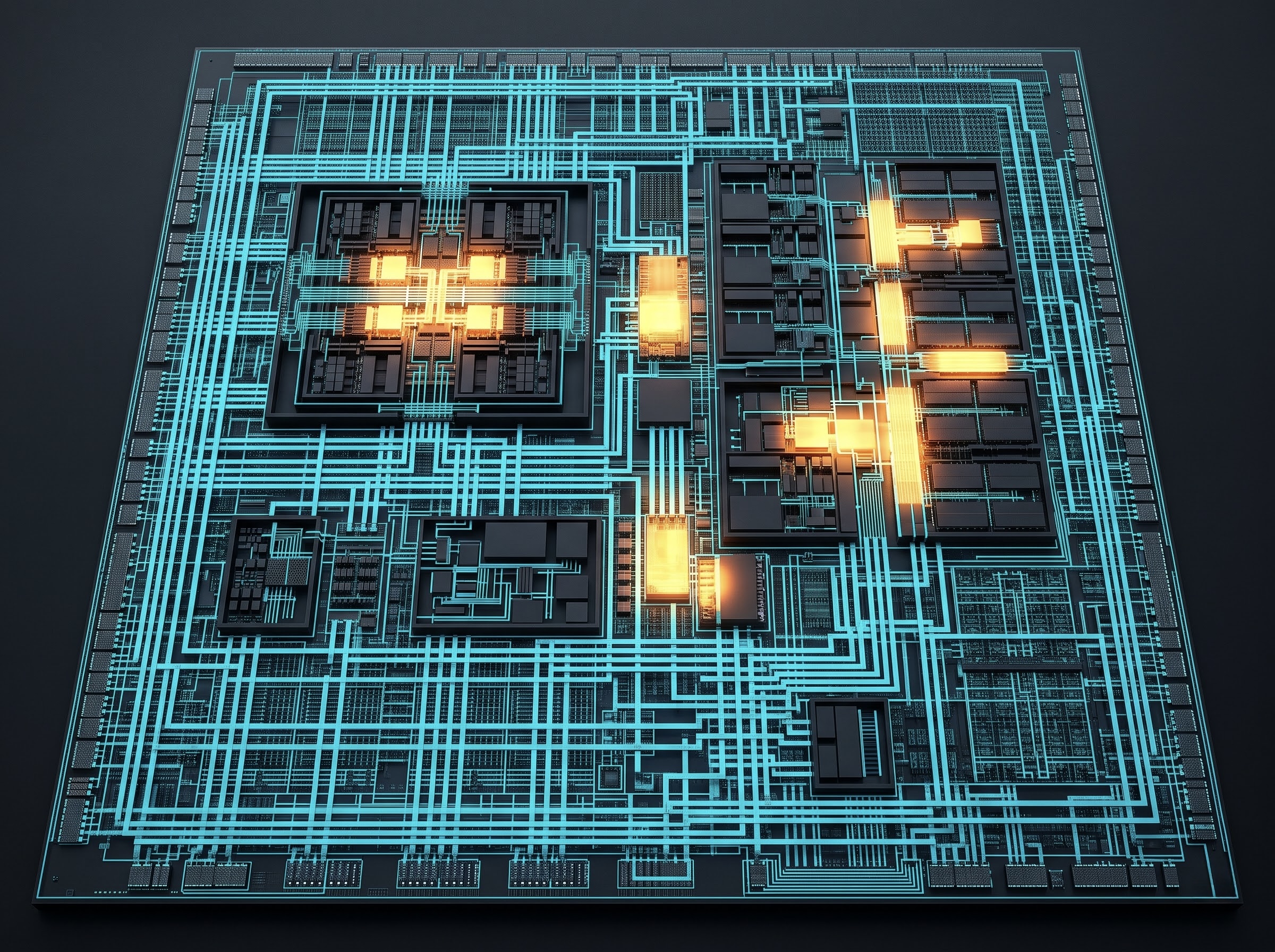
Physical Design transforms the synthesized netlist into a manufacturable silicon layout while meeting power, performance, and area targets.

STA validates timing performance and ensures that all timing paths meet the required operating frequency and performance targets.

Physical Verification ensures the final layout complies with manufacturing rules and accurately represents the intended design.
Embedded Systems engineering focuses on developing software and firmware that control hardware devices, enabling intelligent and connected products.
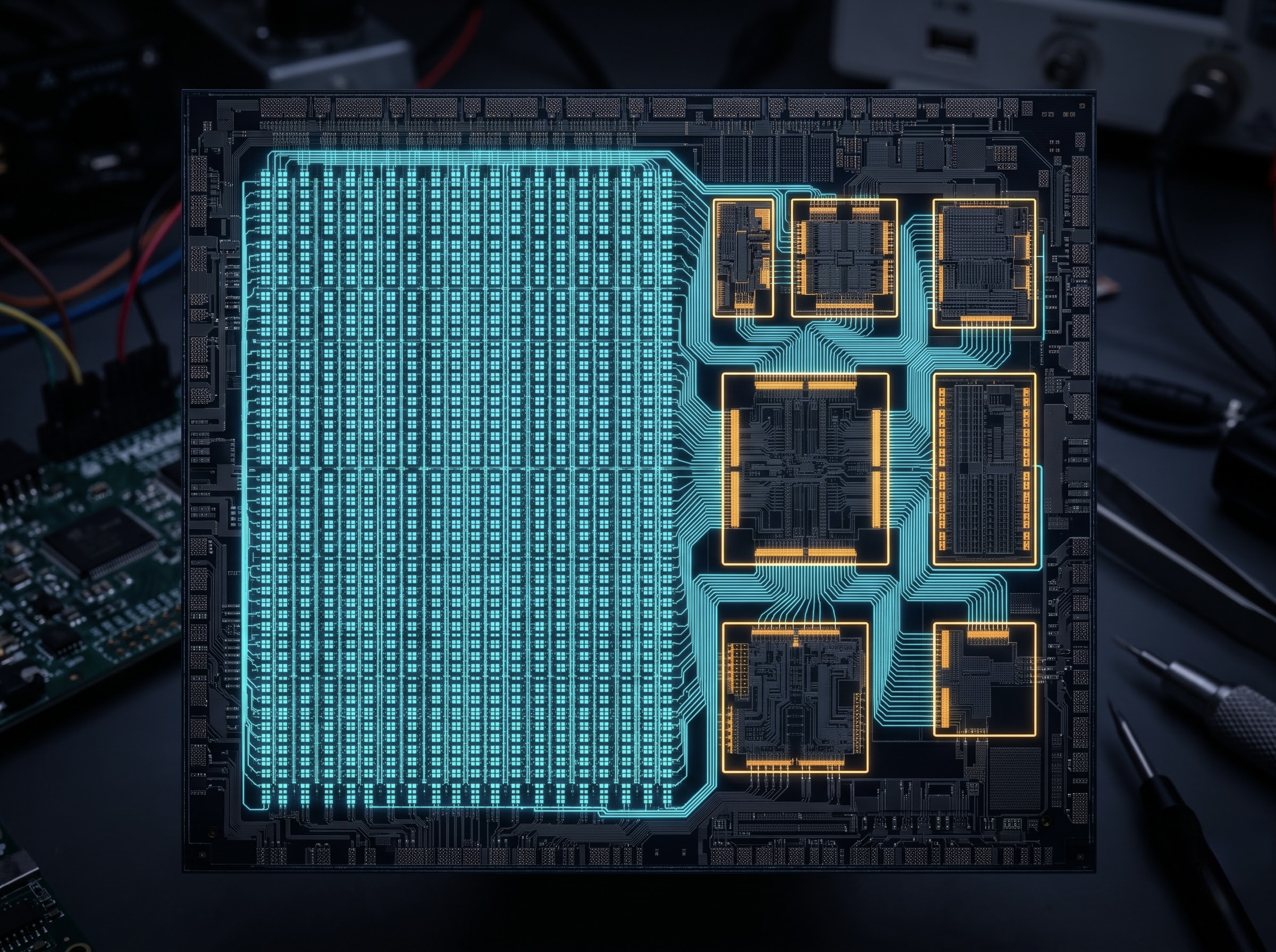
FPGA technology enables rapid prototyping, hardware acceleration, and flexible hardware development.
Spec & architecture
RTL & verification
Physical implementation
Sign-off & tape-out
Bring-up & ramp
Trusted by leading semiconductor and technology companies across the silicon lifecycle.
Clients include Google, Intel, Samsung, Qualcomm, MediaTek, Micron, Cisco, Ethernovia, Appose, Route2SoC, NextGen Silicon, Deft Solutions